


 Designer’s Notebook: What Designers Need to Know About Manufacturing, Part 2
 The Pulse: Drilling Down on Documentation
 Connect the Dots: Designing for Reality: Prioritizing Manufacturability
New Cadence Allegro Enhances Flex and Rigid-Flex Capabilities
May 4, 2016 | Cadence Design Systems, Inc.Estimated reading time: 3 minutes
Cadence Design Systems has unveiled the Allegro 17.2-2016 portfolio, which enables a more predictable and shorter design cycle. The portfolio features comprehensive in-design inter-layer checking technology that minimizes design-check-redesign iterations and a new dynamic concurrent team design capability that accelerates product creation time by up to 50 percent. Utilizing material inlay fabrication techniques, these new capabilities can reduce material costs by up to 25 percent. In addition, embedded Sigrity technology now ensures critical signals meet performance criteria and power integrity (PI) for PCB designers addressing power delivery and IR-drop issues efficiently, eliminating time-consuming iterations with PI experts.
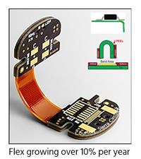
The Allegro portfolio includes key advancements that minimize design iterations and lower overall cost for flex and rigid-flex designs commonly used in automotive, consumer electronics, computing, communications, mobile and wearable applications. These capabilities include:
- Rigid-Flex design enhancements that give designers the ability to specify multiple rigid and flex stack-ups in the same database. This stack-up-by-zone feature can also be used in rigid designs to create material inlay regions leveraging a mix of expensive and inexpensive materials, enabling reduction of material cost by up to 25 percent.
- Unique and comprehensive in-design inter-layer checks for flex and rigid-flex that saves manual effort and ensures all rules for advance flex designs are adhered to, avoiding many design-check-redesign iterations.
- PI for PCB designers that leverages Allegro and Sigrity technologies to provide faster, more reliable access to IR-drop analysis results, enabling PCB designers to efficiently meet power delivery network (PDN) design requirements.
- Interoperable Allegro and Sigrity technologies that provide an easy to use environment, which shortens design and verification time. This is achieved by avoiding unnecessary physical prototype iterations through improved route channel utilization using tabbed routing, new in-design backdrilling rules and efficient sharing of custom return path via structures optimized with Sigrity technology.
- New Native 3D engine that streamlines the system design process and provides improved visualization and collision detection to avoid unnecessary MCAD/ECAD iterations.
The Allegro portfolio now provides synchronous team design capability, which can shorten design time by up to 50 percent for dense designs and increase efficiency by enabling the team to design synchronously. This feature enables PCB designers to achieve maximum productivity by allowing up to five PCB designers to conduct real-time, concurrent PCB design work within the same design database, shortening time to route a dense design by up to 80 percent.
"Due to the nature of our business, flex designs are extremely critical to many of our products, specifically in the mobile and automotive space. The breadth and the depth of enhancements have the ability to significantly improve our PCB design productivity in designing for space-constrained applications," said Greg Bodi, director of System Engineering PCB Layout, Nvidia. "The new inter-layer check capability provides comprehensive in-design, real-time checks, which will save us significant time currently spent doing manual checks after layout is completed on advance flex and rigid-flex designs."
"The latest Allegro release provides many productivity and ease of use improvements," said Dave Elder, PCB Engineering manager at Tait Communications. "In-design inter-layer checks for flex and rigid-flex design is comprehensive and extensible, which can save us 20 to 25 percent time for rigid-flex designs. This will also allow us to retire some homegrown solutions we put in place."
"The new Allegro platform addresses many challenges faced by PCB designers on a daily basis," said Saugat Sen, vice president of R&D, PCB and IC Packaging Group at Cadence. "We continue to provide market-leading solutions with Allegro's extensive Rigid/Flex capabilities coupled with industry-leading power aware Sigrity SI/PI technology to reduce design cycle time for our customers' compact, high-performance products."
About Cadence
Cadence enables global electronic design innovation and plays an essential role in the creation of today's integrated circuits and electronics. Customers use Cadence software, hardware, IP and services to design and verify advanced semiconductors, consumer electronics, networking and telecommunications equipment, and computer systems. The company is headquartered in San Jose, Calif., with sales offices, design centers and research facilities around the world to serve the global electronics industry. More information about the company, its products and its services is available at www.cadence.com.
Share on:


Suggested Items
iNEMI Packaging Tech Topic Series: Role of EDA in Advanced Semiconductor Packaging
04/26/2024 | iNEMIAdvanced semiconductor packaging with heterogenous integration has made on-package integration of multiple chips a crucial part of finding alternatives to transistor scaling. Historically, EDA tools for front-end and back-end design have evolved separately; however, design complexity and the increased number of die-to-die or die-to-substrate interconnections has led to the need for EDA tools that can support integration of overall design planning, implementation, and system analysis in a single cockpit.
Cadence, TSMC Collaborate on Wide-Ranging Innovations to Transform System and Semiconductor Design
04/25/2024 | Cadence Design SystemsCadence Design Systems, Inc. and TSMC have extended their longstanding collaboration by announcing a broad range of innovative technology advancements to accelerate design, including developments ranging from 3D-IC and advanced process nodes to design IP and photonics.
Ansys, TSMC Enable a Multiphysics Platform for Optics and Photonics, Addressing Needs of AI, HPC Silicon Systems
04/25/2024 | PRNewswireAnsys announced a collaboration with TSMC on multiphysics software for TSMC's Compact Universal Photonic Engines (COUPE). COUPE is a cutting-edge Silicon Photonics (SiPh) integration system and Co-Packaged Optics platform that mitigates coupling loss while significantly accelerating chip-to-chip and machine-to-machine communication.
Siemens’ Breakthrough Veloce CS Transforms Emulation and Prototyping with Three Novel Products
04/24/2024 | Siemens Digital Industries SoftwareSiemens Digital Industries Software launched the Veloce™ CS hardware-assisted verification and validation system. In a first for the EDA (Electronic Design Automation) industry, Veloce CS incorporates hardware emulation, enterprise prototyping and software prototyping and is built on two highly advanced integrated circuits (ICs) – Siemens’ new, purpose-built Crystal accelerator chip for emulation and the AMD Versal™ Premium VP1902 FPGA adaptive SoC (System-on-a-chip) for enterprise and software prototyping.
Listen Up! The Intricacies of PCB Drilling Detailed in New Podcast Episode
04/25/2024 | I-Connect007In episode 5 of the podcast series, On the Line With: Designing for Reality, Nolan Johnson and Matt Stevenson continue down the manufacturing process, this time focusing on the post-lamination drilling process for PCBs. Matt and Nolan delve into the intricacies of the PCB drilling process, highlighting the importance of hole quality, drill parameters, and design optimization to ensure smooth manufacturing. The conversation covers topics such as drill bit sizes, aspect ratios, vias, challenges in drilling, and ways to enhance efficiency in the drilling department.