


 Designer’s Notebook: What Designers Need to Know About Manufacturing, Part 2
 The Pulse: Drilling Down on Documentation
 Connect the Dots: Designing for Reality: Prioritizing Manufacturability
Zuken Unveils High-Speed Features for Internet-Connected PCB Design
December 18, 2019 | ZukenEstimated reading time: 2 minutes
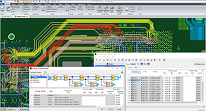
Zuken unveils advanced high-speed design features for its recently launched eCADSTAR connected PCB design platform. eCADSTAR Advanced HS extends eCADSTAR’s connected 3D PCB design capabilities with powerful high-speed routing tools, such as length and delay-based impedance and skew control and comprehensive constraint management capabilities. With the release of eCADSTAR Advanced HS, eCADSTAR is now available in four complementary bundles that can be easily combined to meet individual profiles.
“As products become more complex and connected, high-speed design is a key part of the design and manufacturability of printed circuit boards (PCBs). High-speed components and interfaces are at the heart of today’s smart and internet-connected products, and they demand advanced requirements for layout and routing,” says John Berrie, Signal Integrity Expert, Zuken Tech Center, Bristol. “eCADSTAR Advanced HS delivers those capabilities in an easy to use environment so that PCB designers can deliver exceptional high-speed design quality.”
High-speed PCB design
The need to utilize high-speed design principles is becoming the norm rather than the exception—even if the clock-rates are not in the gigahertz range. Many of today’s common components like DDR3, DDR4 or DDR5 SDRAMs require high-speed PCB design practices to produce high-signal quality. As product performance increases and the need for device connectivity is pervasive, so is the need for high-speed constraint-driven PCB layout techniques.
eCADSTAR Advanced HS
With a consistent user interface from design entry through physical layout and a central constraint browser, eCADSTAR Advanced HS provides powerful built-in capabilities to address the complex details of critical high-speed layout and routing. Constraints can be specified both in the schematic, and the physical design tools, or as design rules stacks eCADSTAR’s built-in constraint browser. eCADSTAR’s high-speed capabilities include:
- Impedance controlled routing: In eCADSTAR, hardware engineers can constrain both single-ended and differential impedance to meet constraints on each board layer.
- Length, delay, and skew based routing: eCADSTAR works with both, length and delay constraints, including built-in simulation for detailed investigation of effects such as signal-to-signal coupling.
- Topology control: High-speed signals need a routing topology that adheres to specified constraints. eCADSTAR enables topology control with a wide selection of templates and instant visualization to make control as fast and reliable as possible.
- Handling of differential signals: In eCADSTAR differential signals can be routed with the assistance of automatic, clean end routing, specific design rules, and constraints.
Configurations and pricing
With modular bundles, eCADSTAR Base, Advanced 3D, Advanced HS, and Ultimate eCADSTAR can be configured in a wide variety of options to fit individual needs. eCADSTAR promotional pricing starts at under £2000 / €2200 EUR / $US2500.
Share on:


Suggested Items
Cadence, TSMC Collaborate on Wide-Ranging Innovations to Transform System and Semiconductor Design
04/25/2024 | Cadence Design SystemsCadence Design Systems, Inc. and TSMC have extended their longstanding collaboration by announcing a broad range of innovative technology advancements to accelerate design, including developments ranging from 3D-IC and advanced process nodes to design IP and photonics.
Ansys, TSMC Enable a Multiphysics Platform for Optics and Photonics, Addressing Needs of AI, HPC Silicon Systems
04/25/2024 | PRNewswireAnsys announced a collaboration with TSMC on multiphysics software for TSMC's Compact Universal Photonic Engines (COUPE). COUPE is a cutting-edge Silicon Photonics (SiPh) integration system and Co-Packaged Optics platform that mitigates coupling loss while significantly accelerating chip-to-chip and machine-to-machine communication.
Siemens’ Breakthrough Veloce CS Transforms Emulation and Prototyping with Three Novel Products
04/24/2024 | Siemens Digital Industries SoftwareSiemens Digital Industries Software launched the Veloce™ CS hardware-assisted verification and validation system. In a first for the EDA (Electronic Design Automation) industry, Veloce CS incorporates hardware emulation, enterprise prototyping and software prototyping and is built on two highly advanced integrated circuits (ICs) – Siemens’ new, purpose-built Crystal accelerator chip for emulation and the AMD Versal™ Premium VP1902 FPGA adaptive SoC (System-on-a-chip) for enterprise and software prototyping.
Listen Up! The Intricacies of PCB Drilling Detailed in New Podcast Episode
04/25/2024 | I-Connect007In episode 5 of the podcast series, On the Line With: Designing for Reality, Nolan Johnson and Matt Stevenson continue down the manufacturing process, this time focusing on the post-lamination drilling process for PCBs. Matt and Nolan delve into the intricacies of the PCB drilling process, highlighting the importance of hole quality, drill parameters, and design optimization to ensure smooth manufacturing. The conversation covers topics such as drill bit sizes, aspect ratios, vias, challenges in drilling, and ways to enhance efficiency in the drilling department.
Elevating PCB Design Engineering With IPC Programs
04/24/2024 | Cory Blaylock, IPCIn a monumental stride for the electronics manufacturing industry, IPC has successfully championed the recognition of the PCB Design Engineer as an official occupation by the U.S. Department of Labor (DOL). This pivotal achievement not only underscores the critical role of PCB design engineers within the technology landscape, but also marks the beginning of a transformative journey toward nurturing a robust, skilled workforce ready to propel our industry into the future.