


 Designer’s Notebook: What Designers Need to Know About Manufacturing, Part 2
 The Pulse: Drilling Down on Documentation
 Connect the Dots: Designing for Reality: Prioritizing Manufacturability
Keysight Delivers Design-to-Test Workflow for High-Speed Digital Designs
September 16, 2022 | Business WireEstimated reading time: 2 minutes
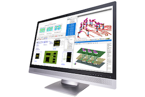
Keysight Technologies, Inc., a leading technology company that delivers advanced design and validation solutions to help accelerate innovation to connect and secure the world, announced PathWave Advanced Design System (ADS) 2023 for high-speed digital (HSD) design with new Memory Designer capabilities for modeling and simulation of next-generation interface standards such as Double Data Rate 5 (DDR5).
As data center throughput climbs, performance expectations of servers and high-performance computing drive the need for new high-density, ultra-fast memory or DDR5 Dynamic Random Access Memory (DRAM). Operating at twice the data rate of DDR4 memory results in shrinking design margins and makes it difficult for hardware designers to optimize printed circuit boards (PCB) to minimize the effects of reflection, crosstalk and jitter. In addition, lower voltages, higher currents and new requirements for equalization within the DRAM receiver create signal integrity challenges that are difficult and costly to troubleshoot.
Keysight’s PathWave ADS 2023 for HSD ensures rapid simulation setup and advanced measurements while providing designers critical insights to overcome signal integrity challenges. Its new Memory Designer quickly constructs parameterized memory buses using the new pre-layout builder, allowing designers to explore system trade-offs that reduce design time and de-risk product development for DDR5, Low-Power Double Data Rate (LPDDR5 / 5x), and Graphics Double Data Rate (GDDR6 / 7) memory systems.
“The biggest takeaway from our first DDR5 design is just how many aspects there are to consider with simulation,” said Lorenzo Forni, PCB design and SI/PI leader at SECO, an Italian industrial group that designs and produces embedded systems and IoT solutions. “You must combine the stack-up analysis, routing geometry and the AMI models. Fortunately, we used Keysight’s Memory Designer for the DDR5 simulation and it's very automated. The configurations are built-in and it's very easy. The setup of the Memory Designer schematic reduced the amount of time needed, and simulation caught many issues during our design process.”
“Keysight has a long history of being on the forefront of channel simulation technology as well as test leadership in memory industry standards bodies including JEDEC,” said Stephen Slater, director of PathWave HSD product management at Keysight Technologies. “We are committed to building the widest portfolio of products and services for DDR enablement, including a complete design-to-test workflow for DDR5 memory from simulation to probing and fixturing. As a result, our HSD design customers experience a more predictive flow and higher confidence at design signoff.”
Keysight’s PathWave ADS 2023 key customer benefits include:
Accurate Simulation and Modeling
- Supports a broad range of next-generation standards: LPDDR4, LPDDR5, GDDR6, GDDR7, HBM2/2E, HBM3, and NAND
- Accurately predicts the closure and equalization of the Data Eye: minimizes impact of jitter, ISI and crosstalk using single-ended I/O (Input-Output) buffer information specification algorithmic modeling interface (IBIS-AMI) modeling with forwarded clocking, DDR bus simulation and accurate electromagnetic (EM) extraction of PCB signal routing
- Shortens time-to-market with a single design environment that enables pathfinding in pre-silicon digital twins to address current integration requirements such as forwarded clocking and timing, IBIS algorithmic modeling interface (IBIS-AMI) modeling and compliance tests and future challenges like single-ended Pulse Amplitude Modulation 4 level (PAM4), for exploration of DDR6
Rapid Simulation Times
- Rapidly generates buses via a parameterized pre-layout builder which enables designers to quickly generate wide buses of memory signals and easily create flexible schematics to explore trade-offs
- Completes simulation up to 80 percent faster: cloud-based high-performance computing (HPC) utilizes parallel processing to accelerate Memory Designer and EM simulation run times
Linking Simulation to Test
- Automates design-to-test workflows with an easy connection between simulation and measurement domains to enable comparison of the stored data against measured results from physical prototypes
Share on:


Suggested Items
iNEMI Packaging Tech Topic Series: Role of EDA in Advanced Semiconductor Packaging
04/26/2024 | iNEMIAdvanced semiconductor packaging with heterogenous integration has made on-package integration of multiple chips a crucial part of finding alternatives to transistor scaling. Historically, EDA tools for front-end and back-end design have evolved separately; however, design complexity and the increased number of die-to-die or die-to-substrate interconnections has led to the need for EDA tools that can support integration of overall design planning, implementation, and system analysis in a single cockpit.
Cadence, TSMC Collaborate on Wide-Ranging Innovations to Transform System and Semiconductor Design
04/25/2024 | Cadence Design SystemsCadence Design Systems, Inc. and TSMC have extended their longstanding collaboration by announcing a broad range of innovative technology advancements to accelerate design, including developments ranging from 3D-IC and advanced process nodes to design IP and photonics.
Ansys, TSMC Enable a Multiphysics Platform for Optics and Photonics, Addressing Needs of AI, HPC Silicon Systems
04/25/2024 | PRNewswireAnsys announced a collaboration with TSMC on multiphysics software for TSMC's Compact Universal Photonic Engines (COUPE). COUPE is a cutting-edge Silicon Photonics (SiPh) integration system and Co-Packaged Optics platform that mitigates coupling loss while significantly accelerating chip-to-chip and machine-to-machine communication.
Siemens’ Breakthrough Veloce CS Transforms Emulation and Prototyping with Three Novel Products
04/24/2024 | Siemens Digital Industries SoftwareSiemens Digital Industries Software launched the Veloce™ CS hardware-assisted verification and validation system. In a first for the EDA (Electronic Design Automation) industry, Veloce CS incorporates hardware emulation, enterprise prototyping and software prototyping and is built on two highly advanced integrated circuits (ICs) – Siemens’ new, purpose-built Crystal accelerator chip for emulation and the AMD Versal™ Premium VP1902 FPGA adaptive SoC (System-on-a-chip) for enterprise and software prototyping.
Listen Up! The Intricacies of PCB Drilling Detailed in New Podcast Episode
04/25/2024 | I-Connect007In episode 5 of the podcast series, On the Line With: Designing for Reality, Nolan Johnson and Matt Stevenson continue down the manufacturing process, this time focusing on the post-lamination drilling process for PCBs. Matt and Nolan delve into the intricacies of the PCB drilling process, highlighting the importance of hole quality, drill parameters, and design optimization to ensure smooth manufacturing. The conversation covers topics such as drill bit sizes, aspect ratios, vias, challenges in drilling, and ways to enhance efficiency in the drilling department.