


 Designer’s Notebook: What Designers Need to Know About Manufacturing, Part 2
 The Pulse: Drilling Down on Documentation
 Connect the Dots: Designing for Reality: Prioritizing Manufacturability
Pulsonix PCB Design Adds 3D Collision Detection for Multi-board and Board Folding in Version 12.0
April 13, 2022 | PulsonixEstimated reading time: 2 minutes
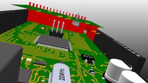
Pulsonix, the Electronic Design Automation (EDA) company delivering technology-leading PCB design solutions, announced the release of Pulsonix version 12.0, which adds new capabilities, significant speed improvements, and highly requested usability enhancements.
“Version 12.0 offers a significant step up for our users in the areas of the PCB design process that they say would benefit them the most, ” said Bob Williams, marketing director for Pulsonix. “The new 3D design features along with 64-bit processing and multi-core support allow our designers to quickly visualize design changes in 3D even with large designs and stacked boards.”
Pulsonix 3D capabilities now include 3D collision detection for both multi-board designs and board folding. This allows designers to visualize boards in a stacked or folded configuration and to verify boards and components fit together in the intended space. Automated clash detection will flag any space violations, and there is a new capability that allows designers to ignore clashes that are intended for known connection points like plugs and sockets.
These new 3D capabilities are integrated into a new consolidated 3D design menu that organizes setup and operation for a more intuitive workflow. This simplifies the interface and enables new functionality while minimizing complexity.
Pulsonix 12.0 is significantly faster due to the new 64-bit implementation and additional multi-threading capabilities to speed up time-consuming functions. Two specific examples are 1) users with large designs will see significant speed ups due to the increased 64-bit address space and multi-threading for library access, and 2) 3D rendering is now multi-threaded meaning 3D viewing and STEP output can be spread across multiple cores and completed in less than half the time.
“Another common request is Dark Mode for the user interface,” added Williams. “Not only does the new Dark Mode option change to a dark background scheme, but we also swap out all toolbar icons to a set that is more compatible with Dark Mode. Whether it's for less eye strain, lower power consumption, or just aesthetics, I'm sure Dark Mode will be a popular feature.”
Additional Rules and DRC checking add new functionality to the Interactive High-Speed option. With new rules such as stub routing length, loop antenna, return path, SMD to corner, and SMD to plane rules, more precision when designing critical advanced circuits can be achieved. Additional enhancements to the editing of differential pair tracks further endorse the precision of Pulsonix.
“With almost 100 documentable additions and changes, Pulsonix Version 12.0 is a significant release with advanced technology and features that directly benefit our customers,” added Williams.
Share on:


Suggested Items
iNEMI Packaging Tech Topic Series: Role of EDA in Advanced Semiconductor Packaging
04/26/2024 | iNEMIAdvanced semiconductor packaging with heterogenous integration has made on-package integration of multiple chips a crucial part of finding alternatives to transistor scaling. Historically, EDA tools for front-end and back-end design have evolved separately; however, design complexity and the increased number of die-to-die or die-to-substrate interconnections has led to the need for EDA tools that can support integration of overall design planning, implementation, and system analysis in a single cockpit.
Cadence, TSMC Collaborate on Wide-Ranging Innovations to Transform System and Semiconductor Design
04/25/2024 | Cadence Design SystemsCadence Design Systems, Inc. and TSMC have extended their longstanding collaboration by announcing a broad range of innovative technology advancements to accelerate design, including developments ranging from 3D-IC and advanced process nodes to design IP and photonics.
Ansys, TSMC Enable a Multiphysics Platform for Optics and Photonics, Addressing Needs of AI, HPC Silicon Systems
04/25/2024 | PRNewswireAnsys announced a collaboration with TSMC on multiphysics software for TSMC's Compact Universal Photonic Engines (COUPE). COUPE is a cutting-edge Silicon Photonics (SiPh) integration system and Co-Packaged Optics platform that mitigates coupling loss while significantly accelerating chip-to-chip and machine-to-machine communication.
Siemens’ Breakthrough Veloce CS Transforms Emulation and Prototyping with Three Novel Products
04/24/2024 | Siemens Digital Industries SoftwareSiemens Digital Industries Software launched the Veloce™ CS hardware-assisted verification and validation system. In a first for the EDA (Electronic Design Automation) industry, Veloce CS incorporates hardware emulation, enterprise prototyping and software prototyping and is built on two highly advanced integrated circuits (ICs) – Siemens’ new, purpose-built Crystal accelerator chip for emulation and the AMD Versal™ Premium VP1902 FPGA adaptive SoC (System-on-a-chip) for enterprise and software prototyping.
Listen Up! The Intricacies of PCB Drilling Detailed in New Podcast Episode
04/25/2024 | I-Connect007In episode 5 of the podcast series, On the Line With: Designing for Reality, Nolan Johnson and Matt Stevenson continue down the manufacturing process, this time focusing on the post-lamination drilling process for PCBs. Matt and Nolan delve into the intricacies of the PCB drilling process, highlighting the importance of hole quality, drill parameters, and design optimization to ensure smooth manufacturing. The conversation covers topics such as drill bit sizes, aspect ratios, vias, challenges in drilling, and ways to enhance efficiency in the drilling department.