


 Designer’s Notebook: What Designers Need to Know About Manufacturing, Part 2
 The Pulse: Drilling Down on Documentation
 Connect the Dots: Designing for Reality: Prioritizing Manufacturability
Siemens Announces New JEDEC Industry Standard for Electronics Cooling Simulation
June 16, 2021 | SiemensEstimated reading time: 2 minutes
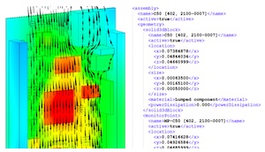
Siemens Digital Industries Software announced the establishment of JEP181—a neutral file, XML-based standard from the JEDEC Solid State Technology Association, which is the global leader in standards development for the microelectronics industry. The JEP181 standard simplifies thermal model data sharing between suppliers and end-users in a single file format called ECXML (Electronics Cooling eXtensible Markup Language).
The new standard was created to meet a significant challenge for electronics manufacturers: as increasingly powerful processors allow companies to pack more performance and functionality into their designs, the effective management of heat dissipation and other thermal factors has become essential to the successful design of their next-generation electronics products. Advanced electronics cooling simulation technologies enable the creation of highly accurate thermal models of new product designs. But the absence of a uniform format for the exchange of thermal simulation data throughout supply chains has created unnecessary duplication of effort and the potential introduction of errors into the stream.
Proposed through the JEDEC JC15 committee, the new JEDEC JEP181 standard simplifies thermal model data sharing. With this universal thermal model sharing standard, electronics manufacturers can reduce the time required to simulate and validate their thermal models.
“The JEP181 standard from JEDEC benefits thermal design engineers by providing wider availability of the key data necessary to validate the thermal performance of today’s advanced designs,” stated Ghislain Kaiser, senior director, Intel Corp. “This standardized format will allow more interoperability between engineering teams, leading to substantial time and cost savings by removing design barriers previously common in thermal engineering.”
Thermal model data availability and sharing is one of the key limiting factors in capitalizing on the benefits of thermal simulation throughout the product design process. Countless hours spent on mining product data sheets for thermal information, or re-implementing 2D engineering drawings within thermal simulation tools, can now be replaced by seamlessly importing commercial 3D simulation tools from software suppliers. The JEP181 standard is ideal for emerging technologies and trends such as miniaturization, 2.5D and 3D semiconductor packaging, and 5G technology-- all of which demand increased power dissipation density.
“As a leader in industrial software solutions, our contribution to the new JEP181 standard can help drive the digitalization of design data to reduce both time and errors for today’s innovative electronics products,” stated Jean-Claude Ercolanelli senior vice president of Simulation and Test Solutions, Siemens Digital Industries Software. “Enabling a seamless digitalized software flow can radically increase the efficiency and accuracy of thermal simulation and thus, enhance the performance and reliability of digital twin prototypes and manufactured products.”
Share on:


Suggested Items
Real Time with… IPC APEX EXPO 2024: My Role as a Technology Solutions Director
05/02/2024 | Real Time with...IPC APEX EXPOPeter Tranitz, senior director of technology solutions at IPC, shares insights into his role as the design initiative lead. He details his advocacy work, industry support, and the responsibilities of the design initiative committee. The conversation also covers the revamping of standards, the IPC Design Competition, and the implementation of design rules in software tools.
Real Time with… IPC APEX EXPO 2024: Ventec Discusses New Pro-bond Family of Advanced Products
05/01/2024 | Real Time with...IPC APEX EXPOChris Hanson, Ventec's Global Head of IMS Technology, outlines the launch of four pro-bond formulas that deliver an outstanding combination of low dissipation factor (Df) with a dielectric constant (Dk) range to maximize the design window for critical PCB parameters. As Chris points out, Pro-bond is designed for low-loss, high-speed applications, while thermal-bond dissipates heat from a component through the board to a heat sink.
IPC's Vision for Empowering PCB Design Engineers
04/30/2024 | Robert Erickson, IPCAs architects of innovation, printed circuit board designers are tasked with translating increasingly complex concepts into tangible designs that power our modern world. IPC provides the necessary community, standards framework, and education to prepare these pioneers as they explore the boundaries of what’s possible, equipping engineers with the knowledge, skills, and resources required to thrive in an increasingly dynamic field.
On the Line With… Talks With Cadence Expert on SI/PI for PCB Designers
05/02/2024 | I-Connect007In “PCB 3.0: A New Design Methodology—SI/PI for PCB Designers,” subject matter expert Brad Griffin, Cadence Design Systems, discusses how an intelligent system design methodology can move some signal and power integrity decision-making into the physical design space, offering real-time feedback.
iNEMI Packaging Tech Topic Series: Role of EDA in Advanced Semiconductor Packaging
04/26/2024 | iNEMIAdvanced semiconductor packaging with heterogenous integration has made on-package integration of multiple chips a crucial part of finding alternatives to transistor scaling. Historically, EDA tools for front-end and back-end design have evolved separately; however, design complexity and the increased number of die-to-die or die-to-substrate interconnections has led to the need for EDA tools that can support integration of overall design planning, implementation, and system analysis in a single cockpit.