-

- News
- Books
Featured Books
- design007 Magazine
Latest Issues
Current Issue
Level Up Your Design Skills
This month, our contributors discuss the PCB design classes available at IPC APEX EXPO 2024. As they explain, these courses cover everything from the basics of design through avoiding over-constraining high-speed boards, and so much more!

Opportunities and Challenges
In this issue, our expert contributors discuss the many opportunities and challenges in the PCB design community, and what can be done to grow the numbers of PCB designers—and design instructors.

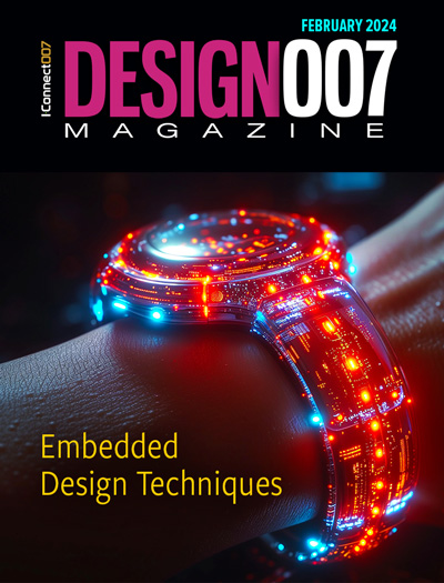
Embedded Design Techniques
Our expert contributors provide the knowledge this month that designers need to be aware of to make intelligent, educated decisions about embedded design. Many design and manufacturing hurdles can trip up designers who are new to this technology.
- Articles
- Columns
Search Console
- Links
- Events
||| MENU - design007 Magazine
Shrinking Silicon, Growing Signal Integrity Challenges
March 9, 2023 | I-Connect007 Editorial TeamEstimated reading time: 2 minutes
What happens when die sizes shrink? As IPC design instructor Kris Moyer explains, quite a bit. Shrinking silicon can mean rising signal speed and rise times, and traditional PCB designers may find themselves dealing with problems formerly only seen by RF engineers.
We asked Kris to discuss the pros and cons of silicon shrinkage and some of the techniques and trade-offs that PCB designers and design engineers need to understand as they find themselves entering the RF arena.
Andy Shaughnessy: This issue focuses on the effects of shrinking silicon on a board’s signal integrity and EMI. So, what do PCB designers need to understand about die shrinkage?
Kris Moyer: Basically, the main thing that happens when you shrink the size of the die is that it shrinks the length of the channel of the transistors inside the die. What that effectively does is it increases the speed of the circuit, meaning it decreases the rise time or the fall time. Then you end up having to start treating your traces, geometries, and transmission lines almost as if they're RF designs.
We've heard for decades that RF designs are their own special little area of black magic, because we start dealing with all these waves and fields and so on. We say in digital design that it's the rise time and not the frequency. Which is the driving force, the key factor, that causes the need for all these high-speed designs? What is the frequency content?
Fourier's theorem says any wave form—square wave, triangle wave, sawtooth wave, or any wave form—can be recreated as a superposition of a sufficient amount of sine waves and cosine waves of sufficiently higher harmonics. Let’s take a fundamental frequency, 1 kilohertz. And you have A1, A3, A5 and A10 kilohertz. You have all these harmonics, we superimpose them, and you end up getting a square wave. Well, how square does that square wave need to be? This is the part that throws a lot of designers off.
When we talk about rise time, we're really talking about the time it takes that square wave, the digital signal, to change from a logic 0 to a logic 1. As the die shrinks, that time also shrinks. About 20 years ago, we were having rise times and fall times in the multiples of nanoseconds—five to 10 nanoseconds. It took that signal five to 10 nanoseconds to change from a logic 0 to a logic 1. I was just looking at one FPGA with rise times as fast as 0.25 nanosecond, and that's at 16 nanometers.
My friends who work in next-generation silicon at some of the big telecom companies are working in 5, 3, and 2 nanometer, and going sub 100 picosecond. Instead of 0.25 nanosecond, it’s 0.1 nanosecond and 0.05 nanosecond rise times. They’re such incredibly fast rise times that the number of harmonics we need to create a vertical square edge that transitions from A0 to A1 that fast means that the frequencies involved in that superposition in that Fourier series are up into the multiple gigahertz of frequency content. That means that you're in the RF frequency range.
To read this entire conversation, which appeared in the February 2023 issue of Design007 Magazine, click here.
Suggested Items
Stan Rak: Elevating the Ideas and Insights of IPC's Thought Leaders Program
04/25/2024 | Stanton Rak, SF Rak CompanyAs a member of the IPC Thought Leaders Program (TLP), I am responsible for identifying knowledge-sharing opportunities that can generate ideas and insights that strengthen the IPC community as well as create a sustainable and lasting future for its members. I am delighted to highlight some of my recent contributions as a member of the TLP.
Alternative Manufacturing Inc. Awarded QML Requalification to IPC J-STD-001 and IPC-A-610
04/24/2024 | IPCIPC's Validation Services Program has awarded an IPC J-STD-001 and IPC-A-610 Qualified Manufacturers Listing (QML) requalification to Alternative Manufacturing Inc (AMI).
IPC Design Competition Champion Crowned at IPC APEX EXPO 2024
04/24/2024 | IPCAt IPC APEX EXPO 2024 in Anaheim, California, five competitors squared off to determine who was the best of the best at PCB design.
Big Win for Defense Production Act Budget Allocation in FY24 Budget
04/23/2024 | I-Connect007 Editorial TeamOne year ago, President Biden issued a determination that chips and packaging are critical for national security. Since that time, much work has been done to continue the conversation in Washington, elevating the importance of the entire chips value chain, and including printed circuit boards and substrates, without which chips cannot operate.
Real Time with... IPC APEX EXPO 2024: A Conversation with IPC's CEO: New Venue, Sustainability, and More
04/23/2024 | Real Time with...IPC APEX EXPOBarry Matties hosts Dr. John W. Mitchell, CEO of IPC, on the final day of IPC APEX EXPO 2024. They discuss the new venue in Anaheim and broach a range of topics, from traffic and booth experiences to workforce development, sustainability, and the CHIPS Act. And they offer advice for newcomers as IPC looks forward to an even better show experience next year.


