-

- News
- Books
Featured Books
- design007 Magazine
Latest Issues
Current Issue
Level Up Your Design Skills
This month, our contributors discuss the PCB design classes available at IPC APEX EXPO 2024. As they explain, these courses cover everything from the basics of design through avoiding over-constraining high-speed boards, and so much more!

Opportunities and Challenges
In this issue, our expert contributors discuss the many opportunities and challenges in the PCB design community, and what can be done to grow the numbers of PCB designers—and design instructors.

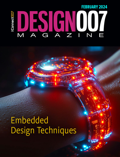
Embedded Design Techniques
Our expert contributors provide the knowledge this month that designers need to be aware of to make intelligent, educated decisions about embedded design. Many design and manufacturing hurdles can trip up designers who are new to this technology.
- Articles
- Columns
Search Console
- Links
- Events
||| MENU - design007 Magazine
Field of Dreams: The Art and Science of Designing with Field Theory
December 23, 2021 | Dan Beeker, NXP SemiconductorsEstimated reading time: 3 minutes
For this issue of Design007 Magazine focusing on the art and science of PCB design, we sought input from Dan Beeker, senior principal engineer of NXP Semiconductors. Dan has spent years teaching designers about the need to focus on the electromagnetic fields around the traces, not the traces themselves, as the late Ralph Morrison advised. We asked Dan to share his thoughts on the art of designing PCBs, and how art and science figure into his views on field theory.
Andy Shaughnessy: We often hear that PCB design is part art and part science, right brain and left brain. Do you think it’s more of one than the other, or does it depend on the design job?
Dan Beeker: I think that the legacy has been more focused on the art side, to make things symmetrical and “pretty.” Now, the science needs to dominate, and those grouped traces need to be separated as much as possible in order to improve signal integrity and reduce crosstalk. The same idea needs to apply to the urge to flood large areas of power conductors to fill in the entire layer. The correct way is to use the vias that connect the power “islands” to the ICs and capacitors, leading to ugly, asymmetrical shapes.
Shaughnessy: Can someone with a great mind for science learn the artistic side of design? That’s one thing that non-degreed designers jokingly say about EEs—that they focus too much on science and not enough on the beauty of the design. What do you think?
Beeker: I am sure that is possible. It is about where you find beauty. I find beauty in visualizing the continuous transmission lines, perfectly controlling the flow of energy, the perspective of symmetry of the two conductors bounding the dielectric. (Yes, I know I am weird.) There is always some beauty resulting from the different colored shapes shown in the layout tools.
Shaughnessy: Does a PCB designer need to have an artistic side to apply the science?
Beeker: I think that one needs to have an abstract side, like Van Gogh or Delaunay—shapes that are defined by their function and connectivity result in the best performance.
Shaughnessy: You’ve been spreading the word about the need for designers and EEs to focus more on fields than on the traces, as many designers were taught. Does this require a designer to have artistic and scientific abilities in order to apply this concept correctly?
Beeker: I believe it goes to trust. It was hard for me to trust the shapes to manage the fields; plumbing connects the sources of energy to the places on the board where it will be used, with enough capacity to do the job. A one-gallon-a-minute hose cannot deliver five gallons a minute. You need a bigger hose or five hoses. The same is true for PCB design.
Shaughnessy: Steve Jobs demanded that the inside of the device look as beautiful as the outside. Are electronics designers and engineers “closet artists” looking for a chance to express themselves?
Beeker: As a goal in itself, that is not always going to yield a good design. Symmetry is a common standard for beauty, and that is rarely present in a good design.
Shaughnessy: Is there anything else you’d like to add?
Beeker: It’s all about the space, which still seems to be the final frontier. If you are not designing the spaces, with today’s products, the cost is severe. Billions of dollars are spent every year by well-meaning design teams on redesigning PCBs, often with very little hope that the new version will be any better than the first. Ralph Morrison said it best:
“Buildings have walls and halls. People travel in the halls not the walls. Circuits have traces and spaces. Energy and signals travels in the spaces not the traces.”
This conversation originally appeared in the December 2021 issue of Design007 Magazine.
Suggested Items
KIC’s Miles Moreau to Present Profiling Basics and Best Practices at SMTA Wisconsin Chapter PCBA Profile Workshop
01/25/2024 | KICKIC, a renowned pioneer in thermal process and temperature measurement solutions for electronics manufacturing, announces that Miles Moreau, General Manager, will be a featured speaker at the SMTA Wisconsin Chapter In-Person PCBA Profile Workshop.
The Drive Toward UHDI and Substrates
09/20/2023 | I-Connect007 Editorial TeamPanasonic’s Darren Hitchcock spoke with the I-Connect007 Editorial Team on the complexities of moving toward ultra HDI manufacturing. As we learn in this conversation, the number of shifting constraints relative to traditional PCB fabrication is quite large and can sometimes conflict with each other.
Standard Of Excellence: The Products of the Future
09/19/2023 | Anaya Vardya -- Column: Standard of ExcellenceIn my last column, I discussed cutting-edge innovations in printed circuit board technology, focusing on innovative trends in ultra HDI, embedded passives and components, green PCBs, and advanced substrate materials. This month, I’m following up with the products these new PCB technologies are destined for. Why do we need all these new technologies?
Experience ViTrox's State-of-the-Art Offerings at SMTA Guadalajara 2023 Presented by Sales Channel Partner—SMTo Engineering
09/18/2023 | ViTroxViTrox, which aims to be the world’s most trusted technology company, is excited to announce that our trusted Sales Channel Partner (SCP) in Mexico, SMTo Engineering, S.A. de C.V., will be participating in SMTA Guadalajara Expo & Tech Forum. They will be exhibiting in Booth #911 from the 25th to the 26th of October 2023, at the Expo Guadalajara in Jalisco, Mexico.
Intel Unveils Industry-Leading Glass Substrates to Meet Demand for More Powerful Compute
09/18/2023 | IntelIntel announced one of the industry’s first glass substrates for next-generation advanced packaging, planned for the latter part of this decade.


