


 Designer’s Notebook: What Designers Need to Know About Manufacturing, Part 2
 The Pulse: Drilling Down on Documentation
 Connect the Dots: Designing for Reality: Prioritizing Manufacturability
American Standard Circuits Utilizes Averatek Process for Medical Technology
December 6, 2021 | American Standard CircuitsEstimated reading time: 1 minute
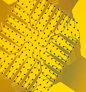
Mr. Anaya Vardya, President and CEO of American Standard Circuits recently discussed how using the Averatek A-SAP™ process allows his company to better service their medical electronics customers.
When commenting on this process Mr. Vardya explained, “Our medical electronics customers depend on us to provide them with the most reliable PCBs possible. When dealing with medical products it is not hyperbole to say that it is always a matter of life or death. With the A-SAP™ manufacturing process ASC can now provide our customers with ultra high-density technology, 25 micron trace and space, and improved reliability, reducing layer counts and micro via lamination cycles, ultimately simplifying the design. Other advantages include improved signal intergrity, aspect ratios greater than 1:1 for metal traces and extremely tight tolerances. Specific to medical technology, this process is not limited to copper conductors and enables the use of gold as a conductive metal to deliver bio-compatibility advantages. In many instances the reduced layer count allows for improved costs which we then pass on to our medical customers. It’s a win-win situation for both of us.”
Visit I-007eBooks to download your copies of American Standard Circuits’ micro eBooks today:
The Printed Circuit Designer’s Guide to... Fundamentals of RF/ Microwave PCBs
The Printed Circuit Designer's Guide to... Flex and Rigid-Flex Fundamentals
The Printed Circuit Designer’s Guide to... Thermal Management: A Fabricator’s Perspective
And be sure to check out Realtime with... American Standard Circuits to learn more!
About American Standard Circuits
American Standard Circuits (ASC) prides itself on being a total solutions provider, manufacturing quality rigid, metal-backed, RF/microwave, flex, and rigid-flex PCBs for the medical, automotive, industrial, defense, and aerospace markets in volumes from test and prototypes to large production orders. ASC has the expertise to provide a wide variety of technologies in a time-critical environment. Their qualifications include AS9100 Rev D, ISO 9001:2015, MIL-PRF 31032, MIL-PRF-55110, MIL-PRF-50884 certification and ITAR registration. In addition to manufacturing in the USA, ASC can transition and manage your PCB requirements to lower cost regions via its qualified supply chain of offshore partners. ASC also holds many key patents for metal bonding processes. For more information about American Standard Circuits' services or to ask one of their technology experts a question go to www.asc-i.com.
Share on:


Suggested Items
Designer’s Notebook: What Designers Need to Know About Manufacturing, Part 2
04/24/2024 | Vern Solberg -- Column: Designer's NotebookThe printed circuit board (PCB) is the primary base element for providing the interconnect platform for mounting and electrically joining electronic components. When assessing PCB design complexity, first consider the component area and board area ratio. If the surface area for the component interface is restricted, it may justify adopting multilayer or multilayer sequential buildup (SBU) PCB fabrication to enable a more efficient sub-surface circuit interconnect.
Insulectro’s 'Storekeepers' Extend Their Welcome to Technology Village at IPC APEX EXPO
04/03/2024 | InsulectroInsulectro, the largest distributor of materials for use in the manufacture of PCBs and printed electronics, welcomes attendees to its TECHNOLOGY VILLAGE during this year’s IPC APEX EXPO at the Anaheim Convention Center, April 9-11, 2024.
ENNOVI Introduces a New Flexible Circuit Production Process for Low Voltage Connectivity in EV Battery Cell Contacting Systems
04/03/2024 | PRNewswireENNOVI, a mobility electrification solutions partner, introduces a more advanced and sustainable way of producing flexible circuits for low voltage signals in electric vehicle (EV) battery cell contacting systems.
Heavy Copper PCBs: Bridging the Gap Between Design and Fabrication, Part 1
04/01/2024 | Yash Sutariya, Saturn Electronics ServicesThey call me Sparky. This is due to my talent for getting shocked by a variety of voltages and because I cannot seem to keep my hands out of power control cabinets. While I do not have the time to throw the knife switch to the off position, that doesn’t stop me from sticking screwdrivers into the fuse boxes. In all honesty, I’m lucky to be alive. Fortunately, I also have a talent for building high-voltage heavy copper circuit boards. Since this is where I spend most of my time, I can guide you through some potential design for manufacturability (DFM) hazards you may encounter with heavy copper design.
Trouble in Your Tank: Supporting IC Substrates and Advanced Packaging, Part 5
03/19/2024 | Michael Carano -- Column: Trouble in Your TankDirect metallization systems based on conductive graphite or carbon dispersion are quickly gaining acceptance worldwide. Indeed, the environmental and productivity gains one can achieve with these processes are outstanding. In today’s highly competitive and litigious environment, direct metallization reduces costs associated with compliance, waste treatment, and legal issues related to chemical exposure. What makes these processes leaders in the direct metallization space?