-

- News
- Books
Featured Books
- design007 Magazine
Latest Issues
Current Issue
Level Up Your Design Skills
This month, our contributors discuss the PCB design classes available at IPC APEX EXPO 2024. As they explain, these courses cover everything from the basics of design through avoiding over-constraining high-speed boards, and so much more!

Opportunities and Challenges
In this issue, our expert contributors discuss the many opportunities and challenges in the PCB design community, and what can be done to grow the numbers of PCB designers—and design instructors.
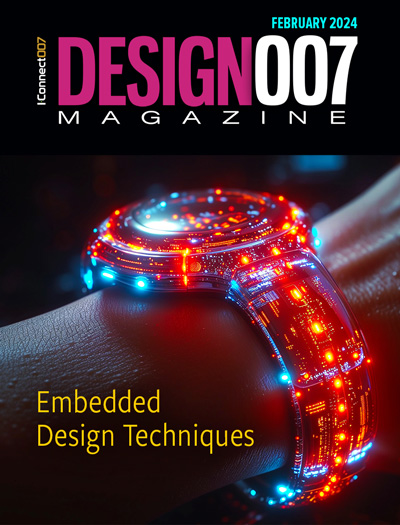
Embedded Design Techniques
Our expert contributors provide the knowledge this month that designers need to be aware of to make intelligent, educated decisions about embedded design. Many design and manufacturing hurdles can trip up designers who are new to this technology.
- Articles
- Columns
Search Console
- Links
- Events
||| MENU - design007 Magazine
Orange County PCEA Lunch ‘n’ Learn Meeting Sept. 1
August 26, 2021 | Scott McCurdy, PCEAEstimated reading time: 1 minute
Join the Orange County Chapter of the Printed Circuit Engineering Association (PCEA) for a virtual Lunch ‘n’ Learn meeting, sponsored by American Standard Circuits.
The meeting will feature two presentations:
First presentation: Next-Gen Line/Space Capability for PCB Designs
Speakers: Anaya Vardya and John Bushie, ASC, and Haris Basit, Averatek
The need for increasingly complex electronics, combined with the obsolescence of larger component packages, is driving innovation to provide alternatives to the traditional subtractive-etch fabrication process that will provide circuit layers reliably, and repeatedly, with trace sizes of 25 micron or finer.
A new process has been developed to handle cutting edge PCB requirements for products of the future. American Standard Circuits is a licensee of Averatek’s A-SAP (Averatek Semi-Additive Process) which enables feature sizes of 25 micron (1 mil) and below, opening new possibilities and options for PCB designers to solve complex design issues. This session will provide an overview of the A-SAP process.
Second presentation: An Overview of Via Fill: Choosing The Right Type For Your Design Application
Speaker: John Bushie, ASC
Many PCBs have requirements for Via Filling yet there are many different options that a designer can chose from depending on their application. Our speaker will present the different types of via fill and plugging methods and describe the pros and cons of the different available options. The types of materials or plating used has an impact on fabrication, so cost implications will be presented with a goal of providing our audience a better understanding of which via filling choice is right for your design project.
Date: September 1, 2021
Time: 11:30 am - 1:00 pm PDT
Where: Virtual meeting at your computer via Zoom while you eat your lunch
Click HERE to register and receive a login.
