-

- News
- Books
Featured Books
- design007 Magazine
Latest Issues
Current Issue
Level Up Your Design Skills
This month, our contributors discuss the PCB design classes available at IPC APEX EXPO 2024. As they explain, these courses cover everything from the basics of design through avoiding over-constraining high-speed boards, and so much more!

Opportunities and Challenges
In this issue, our expert contributors discuss the many opportunities and challenges in the PCB design community, and what can be done to grow the numbers of PCB designers—and design instructors.

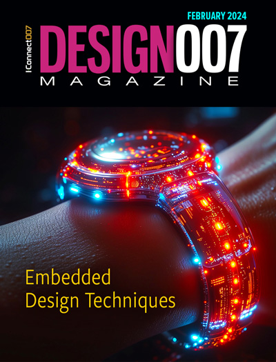
Embedded Design Techniques
Our expert contributors provide the knowledge this month that designers need to be aware of to make intelligent, educated decisions about embedded design. Many design and manufacturing hurdles can trip up designers who are new to this technology.
- Articles
- Columns
Search Console
- Links
- Events
||| MENU - design007 Magazine
Just Ask Heidi: The Biggest Challenge for Design Engineers?
January 5, 2021 | I-Connect007 Editorial TeamEstimated reading time: 1 minute
First, we asked you to send in your questions for Happy Holden, Joe Fjelstad, Eric Camden, John Mitchell, and Tara Dunn in our “Just Ask” series. Now, it’s Heidi Barnes’s turn! Heidi is a senior signal and power integrity engineer at Keysight Technologies. She has written over 20 papers on SI and PI, and she is an active member in developing the new IEEE P370 standard involving interconnect S-parameter quality after fixture removal. Heidi has been awarded five patents and a NASA Silver Snoopy award (each Silver Snoopy pin flies on a space mission first), and she was named DesignCon's 2017 Engineer of the Year. We hope you enjoy “Just Ask Heidi.”
Q: What do you consider to be the biggest challenge for PCB design engineers today?
A: I would have to say impedance, and the fact that electrical signals with fast digital edges and low voltages are much more sensitive to this than ever before. Designers need to start thinking in terms of return paths and impedance to better understand how layout can have an adverse impact on PCB performance. The engineering trade-offs can be quite complex between performance, cost, and risk. Innovative solutions often benefit from the ability of EDA tools to do pre-layout “what-if” simulations using measurement-based models and manufacturing tolerances.
To submit your questions for Heidi, click here.
Suggested Items
Intel Gaudi, Xeon and AI PC Accelerate Meta Llama 3 GenAI Workloads
04/22/2024 | Intel CorporationMeta launched Meta Llama 3, its next-generation large language model (LLM). Effective on launch day, Intel has validated its AI product portfolio for the first Llama 3 8B and 70B models across Intel® Gaudi® accelerators, Intel® Xeon® processors, Intel® Core™ Ultra processors and Intel® Arc™ graphics.
Cadence Unveils Palladium Z3 and Protium X3 Systems
04/18/2024 | Cadence Design SystemsThe Palladium Z3 and Protium X3 systems offer increased capacity, and scale from job sizes of 16 million gates up to 48 billion gates, so the largest SoCs can be tested as a whole rather than just partial models, ensuring proper functionality and performance.
IDTechEx Explores the Role of 3D Cu-Cu Hybrid Bonding in Powering Future HPC and AI Products
04/18/2024 | PRNewswireSemiconductor packaging has evolved from traditional 1D PCB levels to cutting-edge 3D hybrid bonding at the wafer level, achieving interconnecting pitches as small as single micrometers and over 1000 GB/s bandwidth. Key parameters, including Power, Performance, Area, and Cost, are crucial considerations
Northrop Grumman Honors Calumet Electronics with Supplier Excellence Award
04/17/2024 | Calumet ElectronicsNorthrop Grumman Corporation has recognized Calumet Electronics during the company’s 2024 Supplier Excellence Awards for “exceptional performance and unwavering commitment to delivering with excellence.” Calumet is one of 70 suppliers recognized from across the globe. In its award category of “Supplier Strategic Excellence,” Calumet was honored alongside global corporations such as Amazon Web Services, Dell Technologies, and Eaton Corporation.
Micron’s Full Suite of Automotive-Grade Solutions Qualified for Qualcomm Automotive Platforms to Power AI in Vehicles
04/17/2024 | MicronMicron Technology, Inc. announced that it has qualified a full suite of its automotive-grade memory and storage solutions for Qualcomm Technologies Inc.’s Snapdragon® Digital Chassis™, a comprehensive set of cloud-connected platforms designed to power data-rich, intelligent automotive services.


