


 Connect the Dots: Designing for Reality: Prioritizing Manufacturability
 The Shaughnessy Report: Design Takes Center Stage at IPC APEX EXPO
 Elementary, Mr. Watson: Why PCB Design Enthusiasts Should Attend IPC APEX EXPO 2024
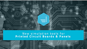
Elsyca Introduces New Simulation Tools for PCB Copper Balancing
April 6, 2020 | ElsycaEstimated reading time: 1 minute
Copper plating is a very complex process that is impacted by the PCB design itself, by the panel layout and by the production configuration.
The ever-increasing complexity of the design and request to deliver in shorter amounts of time are even pushing experts to—and over—their limits.
In order to support the different players in this process, Elsyca has developed a new product suite for the PCB industry. One of the products, Elsyca PCBBalance will not only provide detailed information on the layer thickness distribution, but also optimizes PCB designs/panels for manufacturing through intelligent copper balancing.
In regard to copper balancing and its importance, Rick Hartley, Principal Engineer of RHartley Enterprises commented, “Copper balancing should be done, not only at the panel level in PCB FAB, but every PCB designer should be taught the many benefits of copper balancing and incorporate the concepts into their board designs.”
Elsyca’s PCBBalance simulation software allows users to master quality by providing detailed feedback on the layer thickness distribution and on top of that, also by generating the most performant copper balancing with a single mouse click.
The most critical areas on the panel will be identified, focusing testing resources on where they are most needed.
Key features include:
- DFM
- Identify layer thickness distribution over boards and panels
- Automated and optimized copper balancing
- Identify the most critical holes for post-production quality testing
- Compare different PCB design and panel layouts side by side
- Download copper balancing results
Click on the appropriate link below to find out how this software will help you in your specific role as a PCB Designer, CAM Engineer or Process Engineer.
To learn even more about Elsyca PCBBalance, download a copy of their white paper or find out in one of their webinars how simple it works.
Share on:


Suggested Items
Insulectro’s 'Storekeepers' Extend Their Welcome to Technology Village at IPC APEX EXPO
04/03/2024 | InsulectroInsulectro, the largest distributor of materials for use in the manufacture of PCBs and printed electronics, welcomes attendees to its TECHNOLOGY VILLAGE during this year’s IPC APEX EXPO at the Anaheim Convention Center, April 9-11, 2024.
ENNOVI Introduces a New Flexible Circuit Production Process for Low Voltage Connectivity in EV Battery Cell Contacting Systems
04/03/2024 | PRNewswireENNOVI, a mobility electrification solutions partner, introduces a more advanced and sustainable way of producing flexible circuits for low voltage signals in electric vehicle (EV) battery cell contacting systems.
Heavy Copper PCBs: Bridging the Gap Between Design and Fabrication, Part 1
04/01/2024 | Yash Sutariya, Saturn Electronics ServicesThey call me Sparky. This is due to my talent for getting shocked by a variety of voltages and because I cannot seem to keep my hands out of power control cabinets. While I do not have the time to throw the knife switch to the off position, that doesn’t stop me from sticking screwdrivers into the fuse boxes. In all honesty, I’m lucky to be alive. Fortunately, I also have a talent for building high-voltage heavy copper circuit boards. Since this is where I spend most of my time, I can guide you through some potential design for manufacturability (DFM) hazards you may encounter with heavy copper design.
Trouble in Your Tank: Supporting IC Substrates and Advanced Packaging, Part 5
03/19/2024 | Michael Carano -- Column: Trouble in Your TankDirect metallization systems based on conductive graphite or carbon dispersion are quickly gaining acceptance worldwide. Indeed, the environmental and productivity gains one can achieve with these processes are outstanding. In today’s highly competitive and litigious environment, direct metallization reduces costs associated with compliance, waste treatment, and legal issues related to chemical exposure. What makes these processes leaders in the direct metallization space?
AT&S Shines with Purest Copper on World Recycling Day
03/18/2024 | AT&SThe Styrian microelectronics specialist AT&S is taking World Recycling Day as an opportunity to review the progress that has been made in recent months at its sites around the world in terms of the efficient use of resources: