-

- News
- Books
Featured Books
- design007 Magazine
Latest Issues
Current Issue
Level Up Your Design Skills
This month, our contributors discuss the PCB design classes available at IPC APEX EXPO 2024. As they explain, these courses cover everything from the basics of design through avoiding over-constraining high-speed boards, and so much more!

Opportunities and Challenges
In this issue, our expert contributors discuss the many opportunities and challenges in the PCB design community, and what can be done to grow the numbers of PCB designers—and design instructors.

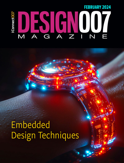
Embedded Design Techniques
Our expert contributors provide the knowledge this month that designers need to be aware of to make intelligent, educated decisions about embedded design. Many design and manufacturing hurdles can trip up designers who are new to this technology.
- Articles
- Columns
Search Console
- Links
- Events
||| MENU - design007 Magazine
Cadence DesignTrue DFM Ecosystem Connects Manufacturers with Customers
September 4, 2018 | Cadence Design Systems, Inc.Estimated reading time: 2 minutes
Cadence Design Systems, Inc. has launched a broad ecosystem with nine initial printed circuit board (PCB) manufacturing partners to enable customers to easily get the partners’ technology files they need to ensure PCB design manufacturability early in the design process. This reduces rework, shortens design cycles, and accelerates new product introduction. Customers have received savings from half to two-thirds fewer technical queries (TQs) from manufacturers when they’ve used the Cadence DesignTrue DFM (design for manufacturability) technology due to using tailor-made spacing, annular ring, copper features and mask rules to assure they are designing the board correctly the first time.
Cadence DesignTrue DFM functionality flags manufacturing rule violations in real time during the PCB layout process with both the Allegro and OrCAD design tools. All other PCB design tools demand designers wait until the design is complete to do DFM signoff on manufacturing outputs, which often requires significant rework and schedule delays.
Nine PCB manufacturers have already become Cadence DesignTrue partners, allowing them to distribute their manufacturing rules to Cadence customers. These include Bay Area Circuits, CircuitHub, Mass Design, Multek, OSH Park, Rocket EMS, Sierra Circuits, Tempo Automation and Würth Elektronik.
“Our goal is to improve PCB designer productivity, and this large ecosystem and new web portals allow our customers to significantly shorten their design cycles with the industry’s first real-time in-design DFM checking,” said Steve Durrill, senior product engineering group director at Cadence. “Instead of manually adding the rules to their PCB design environment, now they can quickly download the appropriate file and update as required.”
By creating new web portals, Cadence is ensuring that customers can access the latest DFM rules from the PCB manufacturers at the start of their design process. Customers can view participating manufacturers and request DesignTrue DFM technology files directly, eliminating the lengthy and error-prone manual entry of hundreds of rules. DFM rules are checked in real time as part of the PCB layout process, reducing the amount of DFM errors found in the manufacturing output. These checks prevent crucial manufacturing errors and limit iterations required to fix such errors. Partners can use the vendor portal to easily distribute rules that match their post-process DFM checks. Cadence users can take advantage of the customer portal to request and receive the rules they need from the manufacturers.
“The Cadence DesignTrue DFM partner program allows us to easily share our PCB manufacturing rules to Cadence customers,” said Dana Korf, senior director Central Manufacturing Engineering and NPI, Multek. “This ensures our customers are designing to our most up-to-date manufacturing constraints, greatly reducing the number of iterations to address DFM errors that we normally see in the PCB signoff process. This will help our customers get their designs done faster, accelerating new product introduction.”
About Cadence
Cadence enables electronic systems and semiconductor companies to create the innovative end products that are transforming the way people live, work and play. Cadence software, hardware and semiconductor IP are used by customers to deliver products to market faster. The company’s System Design Enablement strategy helps customers develop differentiated products—from chips to boards to systems—in mobile, consumer, cloud datacenter, automotive, aerospace, IoT, industrial and other market segments. Cadence is listed as one of Fortune Magazine's 100 Best Companies to Work For. Learn more here.
Suggested Items
Insulectro’s 'Storekeepers' Extend Their Welcome to Technology Village at IPC APEX EXPO
04/03/2024 | InsulectroInsulectro, the largest distributor of materials for use in the manufacture of PCBs and printed electronics, welcomes attendees to its TECHNOLOGY VILLAGE during this year’s IPC APEX EXPO at the Anaheim Convention Center, April 9-11, 2024.
ENNOVI Introduces a New Flexible Circuit Production Process for Low Voltage Connectivity in EV Battery Cell Contacting Systems
04/03/2024 | PRNewswireENNOVI, a mobility electrification solutions partner, introduces a more advanced and sustainable way of producing flexible circuits for low voltage signals in electric vehicle (EV) battery cell contacting systems.
Heavy Copper PCBs: Bridging the Gap Between Design and Fabrication, Part 1
04/01/2024 | Yash Sutariya, Saturn Electronics ServicesThey call me Sparky. This is due to my talent for getting shocked by a variety of voltages and because I cannot seem to keep my hands out of power control cabinets. While I do not have the time to throw the knife switch to the off position, that doesn’t stop me from sticking screwdrivers into the fuse boxes. In all honesty, I’m lucky to be alive. Fortunately, I also have a talent for building high-voltage heavy copper circuit boards. Since this is where I spend most of my time, I can guide you through some potential design for manufacturability (DFM) hazards you may encounter with heavy copper design.
Trouble in Your Tank: Supporting IC Substrates and Advanced Packaging, Part 5
03/19/2024 | Michael Carano -- Column: Trouble in Your TankDirect metallization systems based on conductive graphite or carbon dispersion are quickly gaining acceptance worldwide. Indeed, the environmental and productivity gains one can achieve with these processes are outstanding. In today’s highly competitive and litigious environment, direct metallization reduces costs associated with compliance, waste treatment, and legal issues related to chemical exposure. What makes these processes leaders in the direct metallization space?
AT&S Shines with Purest Copper on World Recycling Day
03/18/2024 | AT&SThe Styrian microelectronics specialist AT&S is taking World Recycling Day as an opportunity to review the progress that has been made in recent months at its sites around the world in terms of the efficient use of resources:


