


 Punching Out: Breaking Out of the Valuation Box
 Happy’s Tech Talk #28: The Power Mesh Architecture for PCBs
 It’s Only Common Sense: Would You Join Your Own Company?
Gold 'Micro Jewels' from 3D Printer Printing Pure Metal Microparts
October 30, 2018 | University of TwenteEstimated reading time: 2 minutes
Thanks to a laser technique that ejects ultra-tiny droplets of metal, it is now possible to print 3D metal structures, not only simple ‘piles’ of droplets, but complex overhanging structures as well: like a helix of some microns in size, made of pure gold. Using this technique, it will be possible to print new 3D micro components for electronics or photonics.
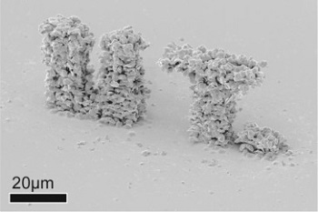
By pointing an ultra-short laser pulse onto a nanometer thin metal film, a tiny metal droplet melts, it is ejected to its target and solidifies again after landing. Thanks to this technique, called laser-induced forward transfer (LIFT), the UT researchers are able to build, drop by drop, a structure with copper and gold microdroplets. The copper acts as a mechanical support for the gold. In their paper in Additive Manufacturing the researchers show, for example, a printed helix: this could act as a mechanical spring or an electric inductor at the same time. This helix is printed with copper around it: together with the helix, a copper ‘box’ is printed. In this way, a droplet that is meant for the new winding that is printed, is prevented from landing on the previous winding. After building the helix, drop by drop and layer by layer, the copper support box is etched away chemically. What remains is a helix of pure gold, no more than a few tens of microns in size.
The laser printing technique: by printing copper and gold in turn, the gold helix initially is surrounded by a copper box. Etching the copper away, results in a free standing helix of pure gold.
Top view (c) of the helix shows that it is threedimensional with a center void. In (b), it is still in the copper box
No Mixing
The volume of the metal droplets is a few femtoliters: a femtoliter is 10-15 liter. To give an impression, a femtoliter droplet has a diameter of little over one micrometer. The way the droplets are made, is by lighting the metal using an ultrashort pulse of green laser light. In this way, the copper and gold structure is built. A crucial question for the researchers was if the two metals would mix at their interface: this would have consequences for the quality of the product after etching. Research shows that there isn’t any mixing. The way a structure is built, drop by drop, results in a surface roughness, which is only about 0.3 to 0.7 microns.
Biomedical
The LIFT technique is a promising technique for other metals and combinations of metals as well. The researchers expect opportunities for materials used in 3D electronic circuit, micromechanic devices and sensing in, for example, biomedical applications. It therefore is a powerful new production technique on a very small scale: an important step towards ‘functionalisation’ of 3D printing.
The research published now, has been done by the departments of Mechanics of Solids, Surfaces and Systems (MS3) and Design, Production and Management (DPM), both part of the Engineering Technology faculty of the University of Twente. The researchers collaborated with DEMCON corporation, a spinoff company of the University of Twente.
Share on:


Suggested Items
MKS’ Atotech to Participate in ECTC
05/10/2024 | MKS’ AtotechAt this year’s 74th IEEE Electronic Components and Technology Conference (ECTC), MKS’ Atotech will present and demonstrate its latest product and service innovations.
The Chemical Connection: Reducing Etch System Water Usage, Part 2
05/02/2024 | Don Ball -- Column: The Chemical ConnectionIn my last column, I reviewed some relatively simple ways to reduce water usage in existing etch systems: cutting down cooling coil water flow, adding chillers to replace plant water for cooling, lowering flow rate nozzles for rinses, etc. This month, I’ll continue with more ways to control water usage in your etcher. Most of these are not easily retrofittable to existing equipment but should be given serious consideration when new equipment is contemplated. With the right combination of add-ons, it is possible to bring the amount of water used in an etch system to almost zero.
Designer’s Notebook: What Designers Need to Know About Manufacturing, Part 2
04/24/2024 | Vern Solberg -- Column: Designer's NotebookThe printed circuit board (PCB) is the primary base element for providing the interconnect platform for mounting and electrically joining electronic components. When assessing PCB design complexity, first consider the component area and board area ratio. If the surface area for the component interface is restricted, it may justify adopting multilayer or multilayer sequential buildup (SBU) PCB fabrication to enable a more efficient sub-surface circuit interconnect.
Insulectro’s 'Storekeepers' Extend Their Welcome to Technology Village at IPC APEX EXPO
04/03/2024 | InsulectroInsulectro, the largest distributor of materials for use in the manufacture of PCBs and printed electronics, welcomes attendees to its TECHNOLOGY VILLAGE during this year’s IPC APEX EXPO at the Anaheim Convention Center, April 9-11, 2024.
ENNOVI Introduces a New Flexible Circuit Production Process for Low Voltage Connectivity in EV Battery Cell Contacting Systems
04/03/2024 | PRNewswireENNOVI, a mobility electrification solutions partner, introduces a more advanced and sustainable way of producing flexible circuits for low voltage signals in electric vehicle (EV) battery cell contacting systems.